I.3. Quantum Dot Infrared Photodetectors
(QDIPs) and Other Device Demonstrations
Our
interests and focus lie in demonstration of methodologies
for, and realization of, the highest quality electronic
and optoelectronic devices of the time. Our contributions
cover:
(a) Quantum Dot Infrared Photodetectors (QDIPs)
[Current Focus]
(b) Quantum Dot Lasers
(c) Heterojunctions and Quantum Wells
(a)
Quantum Dot Infrared Photodetectors (QDIPs):
Development of high performance infra-red (IR) detectors
in the range of mid-wavelength IR (MWIR, 3-5 micron)
and long-wavelength IR (LWIR, 8-12 micron) attract considerable
interest for variety of fields, such as biomedical applications
(e.g., cancer detection), military applications (e.g.,
intercontinental ballistic missile defense), and night
vision, etc. Amongst a few types of IR detectors in
these wavelength ranges, a QDIP has several advantages
over other IR detectors (e.g., quantum well infrared
photodetectors (QWIPs) or HgCdTe (MCT) detectors) because
of unique electronic properties in QDs in which electrons
are 3-dimensionally confined. For instance, QDs shows
much higher absorption of the normal incident photons
than QWs, and are expected to have higher quantum efficiency
owing to long carrier lifetimes of excited electrons,
which, in turn, will reduce dark current to enable the
high temperature operation of IR detectors.
|
 |
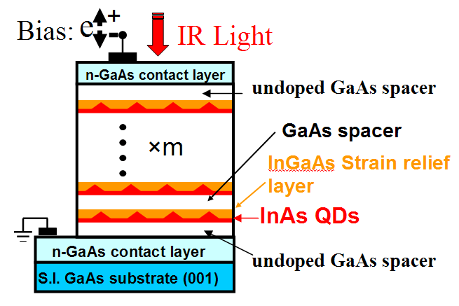
| Figure
1 Schematic structure of InAs/InGaAs/GaAs
QDIP. |
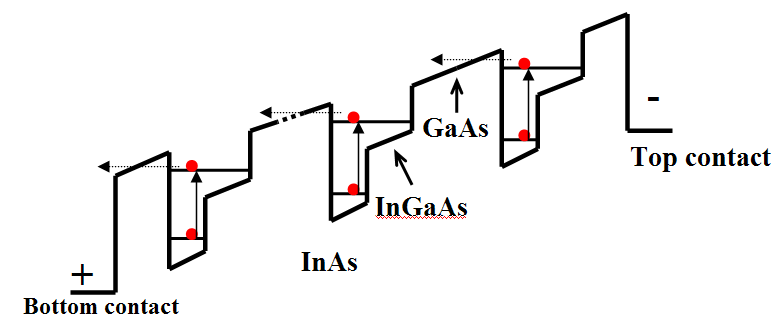
Figure
2 Schematic operation principle of
InAs/InGaAs/GaAs QDIP. |
We have been one of the leading research groups in the
field of QDIPs to have presented comprehensive studies
of QDIP characteristics and its performances from structural
aspects to device aspects on the strength of our accumulated
knowledge of QD properties in terms of their growth kintics,
structural properties, and optical properties under the
collaboration with Prof. Joe Campbell's group (Univ. Virginia).
We have shown one of the first demonstrations of normal
incidence response of QDIP [26-28] with dot-in-well
(DWELL) structure [27,28]. Utilizing
our unique method to selectively manipulate a particular
QD energy level [I.1.(b)(ii)77], voltage
controllable two-color QDIP [29, 30, 32] and
one of the best LWIR QDIP [I.1.(b)(ii)76, 33, 35] have been
demonstrated, as well as we shed light on the interconnections
between QD energy structures and QDIP device characteristics
[26-35].
 |
|
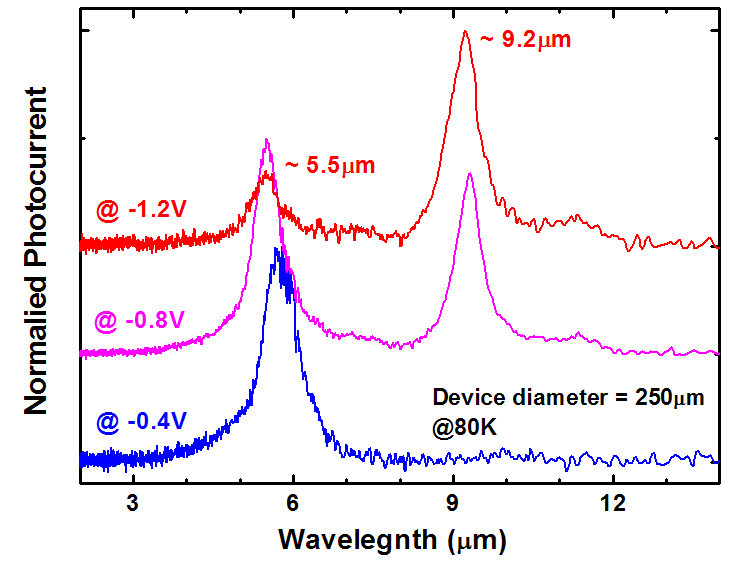
| Figure
3 Demonstration of voltage tunable
two-color photoresponse. |
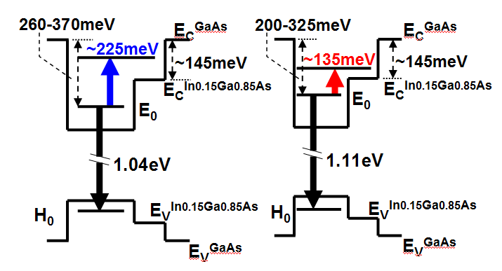
Figure
4 Energy levels of QDs in voltage tunable
two-color QDIP. |
On top of the above extensive studies on QDIP, we are
currently tackling on a remaining challenge in the field
of QDIP and also in other QD devices, that is realization
of rightly doped high quality (low defect density) multiple
QD (MQD) structures. Since SAQDs are inherently strained,
many number of QD layers give rise to accumulated strain
in the structure, which eventually introduces dislocations
and degrades QD optical properties and electronic properties
of MQD structures. At the same time, as the MQD structure
become thicker, doping condition needs to be refined accordingly
to manipulate QD energy levels with respect to Fermi energy
to optimize electron occupancy in QDs.
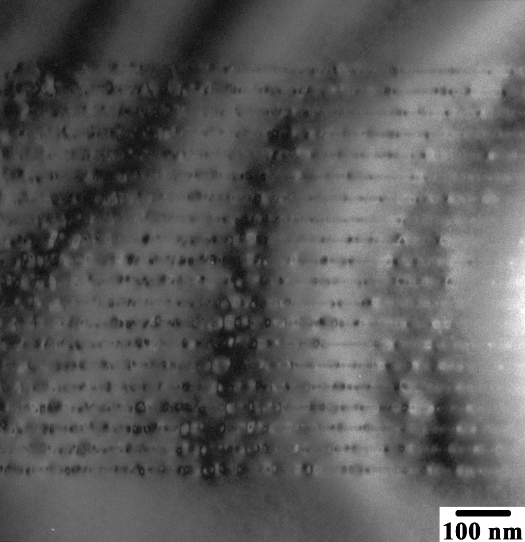
So far we have created 20-layer of MQD structure with
a minimal defect density by utilizing strain relief InGaAs
layer and unimodal shallow distribution of InAs 3D islands.
Figure 5 shows a cross-sectional TEM image (dark field,
g = (220)) of 20 stacks of 2.0ML InAs QDs capped with
20ML InGaAs and 130ML GaAs. QD formation is clearly observed
up to the 20th QD layer, and its density is constant throughout
entire 20 layers. No dislocation is observed within the
examined area. This indicates the dislocation density
< 107 /cm2.
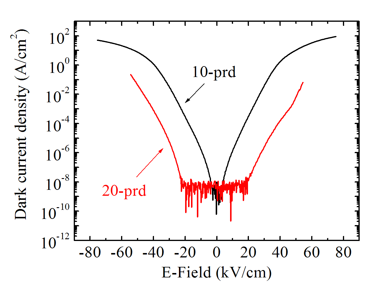
This high quality 20-period QDIP shows much lower dark
current and also lower photocurrent than a 10-period QDIP
(Figure 6) by ~3 order of magnitude, which implies that
lower electron density in MQD region of the 20-period
QDIP. We have attributed this low electron density to
its higher built-in potential in the band bending, which
makes QD energy levels far above Fermi energy with respect
to kBT, from the estimation of the QDs ionization energy
and activation energy deduced from temperature dependent
photocurrent and dark current. We have also studied that
various doping conditions such as n-p-n structure or thicker
spacer layers can reduce dark current significantly (by
~9 order of magnitude), which can be also understood from
the energy level relationships between QD energies and
Fermi energy.
 |
 |
| Figure
5 Cross sectional TEM image of 20-period
QDIP |
Figure
6 Dark current of 10- and 20-period
QDIP |
(b)
Self Assembled Quantum Dots:
We
have demonstrated one of the first quantum dot lasers
in 1996. For details, see [24].
(c)
Heterojunctions and Quantum Wells:
Inverted
HEMTs (high electron mobility transistors, 1988) [1], high power MISFETs
(1992) [4,5], high peak-to-valley
ratio and high peak current density RTDs (resonant tunneling
diodes, 1990) [6,9], high contrast
ratio normal and inverted-geometry multiple quantum
well (MQW) spatial light modulators (SLMs 1989-91) [10,11,14,15,16,18,20]
the first integrated RTD, FET, and SLM based opto-electronic
switch (1992) [22], the
first monolithically integrated heterojunction phototransistor
and semiconductor spatial light modulator [16].
For more information,
click on the highlighted areas.
Research Platforms
Back
to Top
|