A New Paradigm for Solar Energy Conversion: Non-Radiative
Energy Transfer.
Historically, the earliest photovoltaic
solar cells were investigated in silicon p-n junction devices
[1] where the absorption and the created electron-hole pair
separation and transport are processes that occur in the
same medium. With the development of semiconductor epitaxial
deposition techniques, the silicon pn junction solar cells
have been augmented with III-V compound semiconductor multiple
quantum well based solar cells [2] which exhibit the highest
efficiencies although remain also the most expensive to
produce.
Low cost solar cell with organic
absorbers have been and are continuing to be exploited but
the high exciton binding energies typical of such materials
requires their mixing with an appropriately energy-aligned
different material, inorganic or organic, to create internal
heterojunctions at which the photo-generated exciton can
be split into its electron and hole components for subsequent
collection. These have come to be known as excitonic solar
cells [3-6] and in the current implementations of these
the separated electrons and holes end up in two different
media for transport and collection. These media have so
far been ones with very low charge carrier motilities, which
is a major contributing factor to their hitherto low overall
energy conversion efficiency.
Overcoming or bypassing the bottlenecks
of charge carrier extraction and transport to collecting
electrodes will constitute a major step forward in the quest
for the realization of efficient and cost effective solar
energy converters. We have thus introduced
an new paradigm for solar energy conversion. To
learn about this new paradigm see below
(or read our full paper: Siyuan Lu and Anupam Madhukar,
"Nonradiative Resonant Excitation Transfer from Nanocrystal
Quantum Dots to Adjacent Quantum Channels", Nano Letters,
7, 3443-3451 (2007). )
Our
New Solar Cell Paradigm
In the Madhukar group, we are investigating
a new solar cell architecture that bypasses the limitations
of charge carrier extraction and transport by utilizing nonradiative
dipole-dipole coupling for direct
transfer of energy (NRET) from the excitons created in the
solar absorber to high charge carrier mobility transport channels.
In this new solar cell architecture,
shown schematically in figure 1 below, the excitons are created
by light absorption in nanocrystal quantum dot absorbers and
their energy transferred nonradiatively to an adjacent
high carrier mobility transport medium via direct dipole-dipole
interaction between the NCQD and the adjacent transport channel
states. The tranfer rate is given by the Forster expression
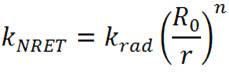
in which kNRET
is the nonradiative energy transfer rate,
krad is the radiative
decay rate, R0
the Forster Critical Radius, r
is the separation between dipoles, and
n depends on the dimensionality of the
acceptor. This mechanism is distinct from those employed
in solar cells of any type (excitonic or otherwise)
so far. Semiconductor quantum wells and quantum or nanowires
are known to provide high carrier mobility channels [7]. Such
channels, quantum wells or wires, are provided by the technology
of the planar or spatially-patterned epitaxial [8-10] quantum
wells and wires (Fig.1a) or chemically templated [11, 12]
wires (nano or quantum) formed perpendicular to the substrate
(Fig.1b). Common to all such architectures, the fundamental
physical process to be examined and established then is the
controlled nonradiative transfer of excitation energy
from the NCQD absorbers to nearby quantum wells and wires.
We emphasize that this process is separate from the break-up
of the exciton at a heterojunction and attendant carrier (electron
or hole) transfer to a transport channel as is the case with
current excitonic solar cells, or radiative energy transfer
to the channel.
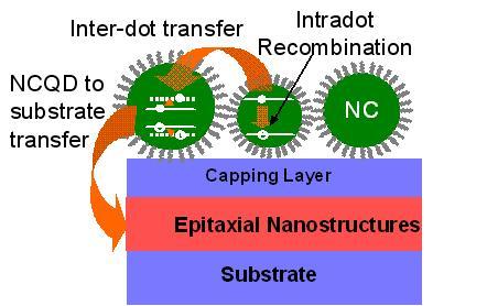 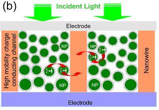
Figure 1. Schematic showing a new solar cell architecture
utilizing nonradiative coupling between dipoles for
direct transfer of energy from the excitons created in the
light absorber to (a) quantum well (b) nanowire high mobility
charge carrier transport channels.
To assess the
viability of hte new approach, we have measured the nonradiaitve
energy transfer rate between nanocrystal quantum dots and
adjacent quantum well, as described below.
Energy transfer in hybrid nanocrystal quantum
dot / adjacent quantum well systems
For efficient nonradiative transfer
of energy, appropriate matching of the absorption and emission
spectra of the donor and acceptor species and their separation
is a critical consideration [13]. For our studies, PbS NCQDs
are employed as the absorbers (donors) and an appropriately
designed adjacent InGaAs quantum well buried in GaAs matrix
provides the high mobility charge transport channel for accepting
the resonantly transferred exciton energy in the form of electron
and hole. To shed light on the time scale and efficiency of
excitation transfer from the PbS NCQD into the InGaAs near
surface quantum well, we have examined the time resolved behavior
of the luminescence decay from the NCQDs adsorbed on quantum
well containing substrates and compared it to the behavior
on control substrates without the buried quantum well.
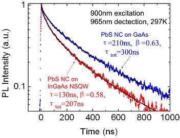
Fig. 2. Time resolved PL of PbS NCs on passivated GaAs
(blue) and on passivated NSQW (Red). Excited at 900nm (below
GaAs bandgap) and detected at 965nm (PbS PL peak). TRPL curves
are fitted using stretched exponential function.
Figure 2 shows the room temperature
time decay behavior of the luminescence peak of the NCQDs
at 965nm. Note the considerably fast decay time of ~207ns
in the presence of the quantum well as compared to the ~300ns
decay time on the GaAs control substrate. The reduction of
the NCQD PL decay time from ~300ns to ~207ns is the manifestation
of the opening of an excitation transfer channel provided
by the one-dimensionally confined states of the quantum well
(Fig.2). From the difference between these two measured decay
times, we calculate the nonradiative transfer rate to be ~
1/(690ns), ~1.4 times faster than their radiative decay rate
~ 1/(960ns) measured for the NCQDs dispersed on a glass substrate.
This means for a nanocrystal of 100% quantum yield, the efficiency
of the nonradiative transfer from the NCQD to the quantum
well is ~60% for the 8.2 nm center-to-center separation of
the PbS NCQDs adn the InGaAs QW in these experiments. The
transfer efficiency is expected to be further improved by
reducing the distance between the NCQDs and the NSQW.
For a full description
of the findings, see our paper:
Siyuan Lu, Anupam Madhukar, "Nonradiative Resonant Excitation
Transfer from Nanocrystal Quantum Dots to Adjacent Quantum
Channels", Nano Letters, 7, 3443-3451 (2007). [CLICK
HERE]
Charge
Carrier Generation and Photocurrent in Silicon Nanowires by
NRET from Adjacent Quantum Dots
To demonstrate the feasibility of using energy
transfer to generate current in high mobility transport channels,
we have measured the time resolved photocurrent in silicon
nanowires - PbS QD hybrid structures as represented in figure
3a below. Photocurrent measurements for devices with and without
QDs are shown in figure 3b. The electron-hole pairs generated
in the silicon nanowires due to direct photon absorption in
the nanowires will be swept away extremely rapidly by a modest
electric field across the wires. By contrast, the NRET time
being several hundred nanoseconds [14], its contribution to
the photocurrent will occur on a similarly long time scale,
thus separating the contribution to the total measured photocurrent
into its two components, those electrons and holes generated
owing to NRET, as shown in the blue curve in figure 3c, and
those generated due to direct absorption in nanowires, as
shown in the black curve in figure 3c. Integrating the curves
in figure 3c shows that the contribution to current from NRET
can be three times greater than that from direct absorption
in the nanowires.
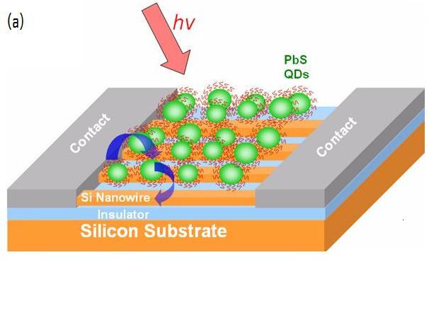 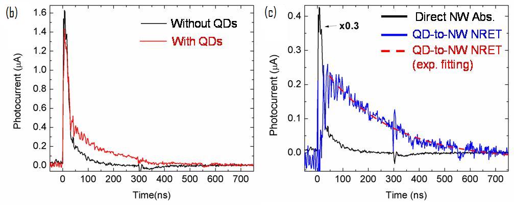
Figure 3: (a) Schematic of silicon nanowire
arrays with PbS QDs used in time resolved photocurrent measurements.
(b) Measured photocurrent for nanowire array wth (red) and
without PbS QDs (black) . (c) Components of photocurrent due
to direct absorption in nanawires (black) and photocurrent
from PbS QD to nanowire energy tranfer (blue).
For a full description,
see our paper:
S. Lu, Z. Lingley, T. Asano, D. Harris, T. Barwicz,
S. Guha, and A. Madhukar, " Photocurrent Induced by Nonradiative
Energy Transfer from Nanocrystal Quantum Dots to Adjacent
Silicon Nanowire Conducting Channels: Towards a New Solar
Cell Paradigm" Nano Lett., 9 , 4548-4552 (2009) [CLICK
HERE]
Enhanced
Interdot Energy Transfer by Reduction
of QD-QD Separation by
Cation-Ligand Exchange
Efficient collection of current requires that
energy from light absorbed in QDs many layers away from the
quantum well or wire surface can be efficiently transfered
dot-to-dot to eventually be transfered from a QD into the
well/wire. To enhance interdot energy transfer we have developed
a method of ligand exchange that allows for control and reduction
of the separation between adjacent PbS QD when the QDs are
in densely packed solids. Our ligand exchange is unique in
that is utilizes lead cation - carboxylate ligands as exchange
units rather than plain ligands as is most commonly used,
and the value of this apporach is that it does not significantly
degrade the quantum efficiency of the PbS quantum dots. Exchanging
the relatively long oleate ligands on as-grown PbS QDs with
shorter dodecatoate and octanoate ligands lead to a decrease
in QD-QD spacing and an increase in the interdot energy transfer
rate, kNRET.
In fact, we demonstrated that the energy transfer rate depends
on the inverse sixth power (n =6 for
QD to QD energy transfer) of interdot sepration, r,
as expected from the Forster expression above.
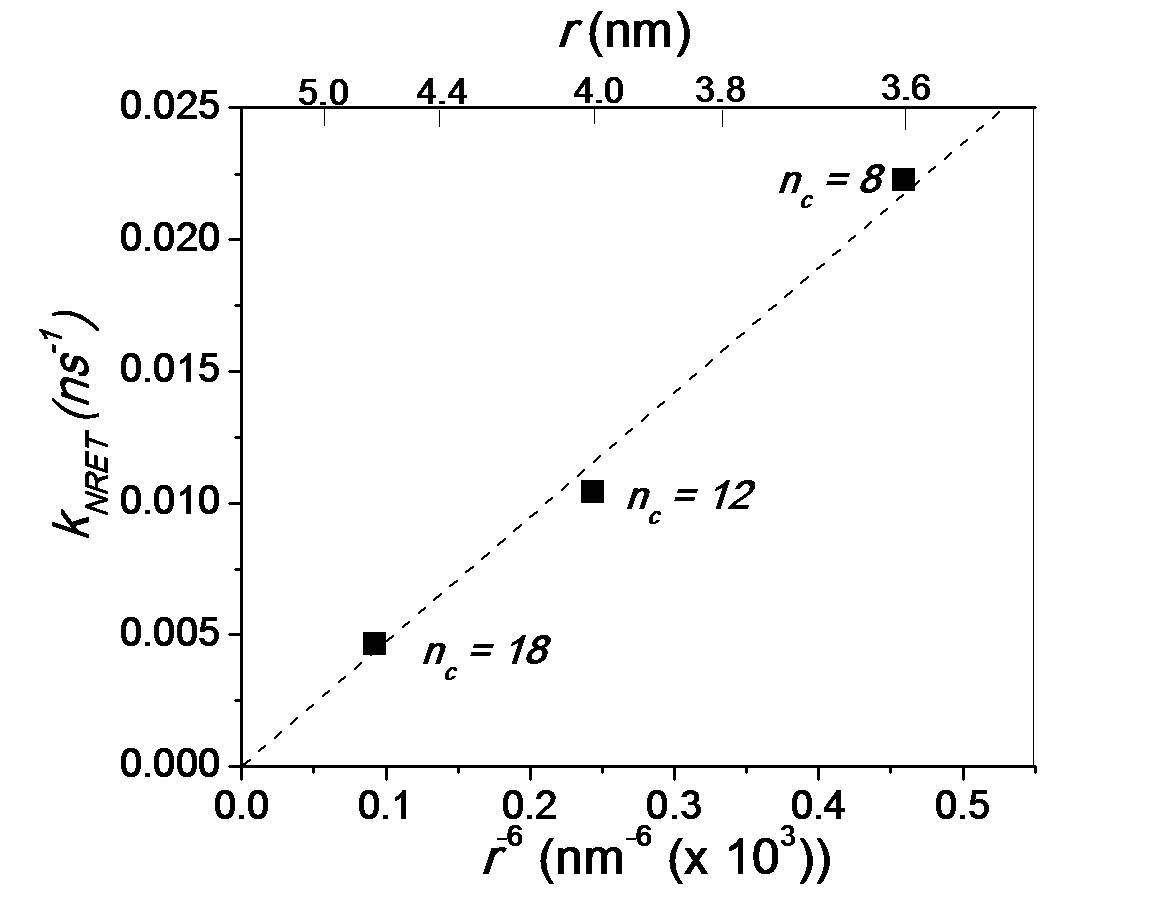
Figure 4: Interdot energy transfer rate, kNRET,
as a function of QD-QD separation, r,
to the inverse sixth power. nc
refers to the number of carbon atoms in the carboxylate ligand
attached to the QD surface.
For a full description,
see our paper:
Z. Lingley, S. Lu. and A. Madhukar, "A
High Quantum Efficiency Preserving Approach to Ligand Exchange
on Lead Sulfide Quantum Dots and Interdot Resonant Energy
Transfer" Nano Lett., 11, 2887-2891 (2011) [CLICK
HERE]
References:
[1] Shockley, W.; and Queisser, H. J.; Jour. App. Phys. 1963,
32, 510-519.
[2] King, R. R.; Law, D. C.; Edmondson, K. M.; Fetzer, C.
M.; Kinsey, G. S.; Yoon, H.; Sherif, R. A.; Karam, N. H.;
Appl. Phys. Lett., 2007, 90, 183516.
[3] Oregan, B.; Gratzel, M.; Nature, 1991, 353, 737-740.
[4] Hoppe, H.; Sariciftci, N. S.; J. Mater. Res. 2004, 19,
1924-1945.
[5] Kim, J. Y. ; Lee, K. ; Coates, N. E. ; Moses, D. ; Nguyen,
T. Q. ; Dante, M. ; Heeger, A. J. ; Science 2007, 317, 222-225.
[6] Nozik, A. J. Physica E, 2002, 14, 115; Gur, I.; Fromer,
N. A.; Alivisatos, A. P.; J. Phys. Chem. B 2006, 110, 25543-25546.
[7] Weisbuch, C. Fundamental properties of III-V semiconductor
two-dimensional quantized structures: The basis for optical
and electronic device applications, Ch.1 in Semiconductors
and Semimetals: Application of Multiquantum Wells, Selective
Doping, and Superlattices, Ed. R. Dingle, Academic Press,
New York, (1987); Interfaces, Quantum Wells, and Superlattices,
Eds, C. R. Leavens and R. Taylor Plenum, New York, (1988).
[8] Madhukar, A.; Thin Solid Films, 1993, 231, 8-42.
[9] Konkar, A.; Madhukar, A.; Chen, P.; Appl. Phys. Lett.,
1998, 72, 220-222.
[10] Kiravittaya, S.; Heidemeyer, H.; Schmidt, O. G.; Physica
E, 2004, 23, 253-259.
[11] Westwater, J.; Gosain, D. P.; Tomiya, S.; Usui, S.; Ruda,
H. J.; Vac. Sci. Technol. B, 1997, 15, 554-557.
[12] Dick, K. A.; Deppert, K.; Karlsson, L. S.; Wallenberg,
L. R.; Samuelson, L.; Seifert, W.; Advanced Functional Materials,
2005, 15, 1603-1610; Zhong, Z. H.; Qian, F.; Wang, D. L.;
Lieber, C. M.; Nano Lett., 2003, 3, 343-346; Kim, Y.; Joyce,
H. J.; Gao, Q.; Tan, H. H.; Jagadish, C.; Paladugu, M.; Zou,
J.; Suvorova, A.; Nano Lett., 2006, 6,599 - 604.
[13] Förster, Th.; Annu. Rev. Phys., 1948, 2, 55-75;
Förster, Th.; Discuss. Faraday Soc., 1959, 27, 7-17.
[14] Lu, S.; Madhukar, A.; Nano Lett. 2007, 7, 3443-3451.
|