UHV
Interconnected Growth & In-Situ Processing, &
Characterization system:
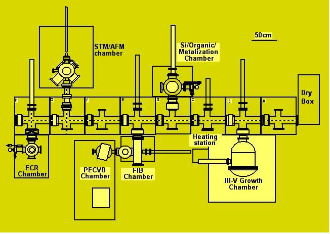
MBE
Chamber:
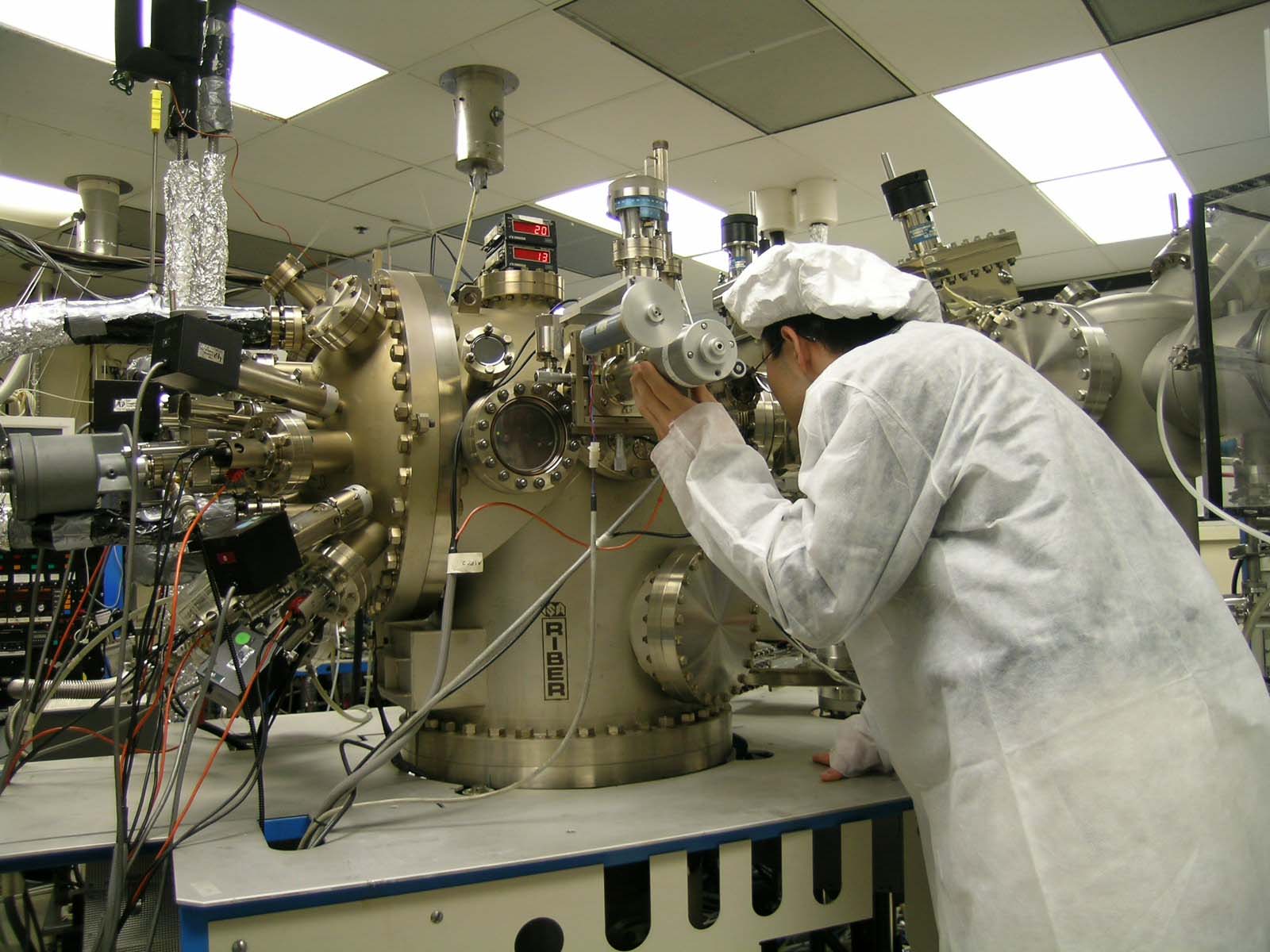
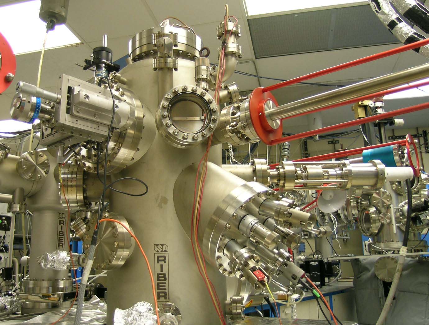
The MBE chamber is the heart of the Integrated UHV interconnected
system and is used for fabrication of advanced III-V
(Ga, Al, In arsenides) epitaxical nanostructures (quantum
well, wires, and dots) and state-of-art devices (lasers,
photodetectors, modulators, transistors). A reflection
high-energy electron diffraction (RHEED) system is integrated
on to the chamber that allows in-situ diagnostics and
real-time control on epitaxical growth. The chamber
has standard Knudsen effusion cells for deposition of
Ga, In, Al, and As. Si and Be K-cells are available
for doping of the structures. Additionally, a water-cooled
Arsenic valved cracker is installed on the chamber.
Substrate temperature is measured using an IR pyrometer.
A quadropole mass-analyzer is used to monitor the background
gas species in the chamber. The combination of cryopump,
ion pump, and titanium sublimation pump on the chamber
achieves base pressure in the low E-10 torr range.
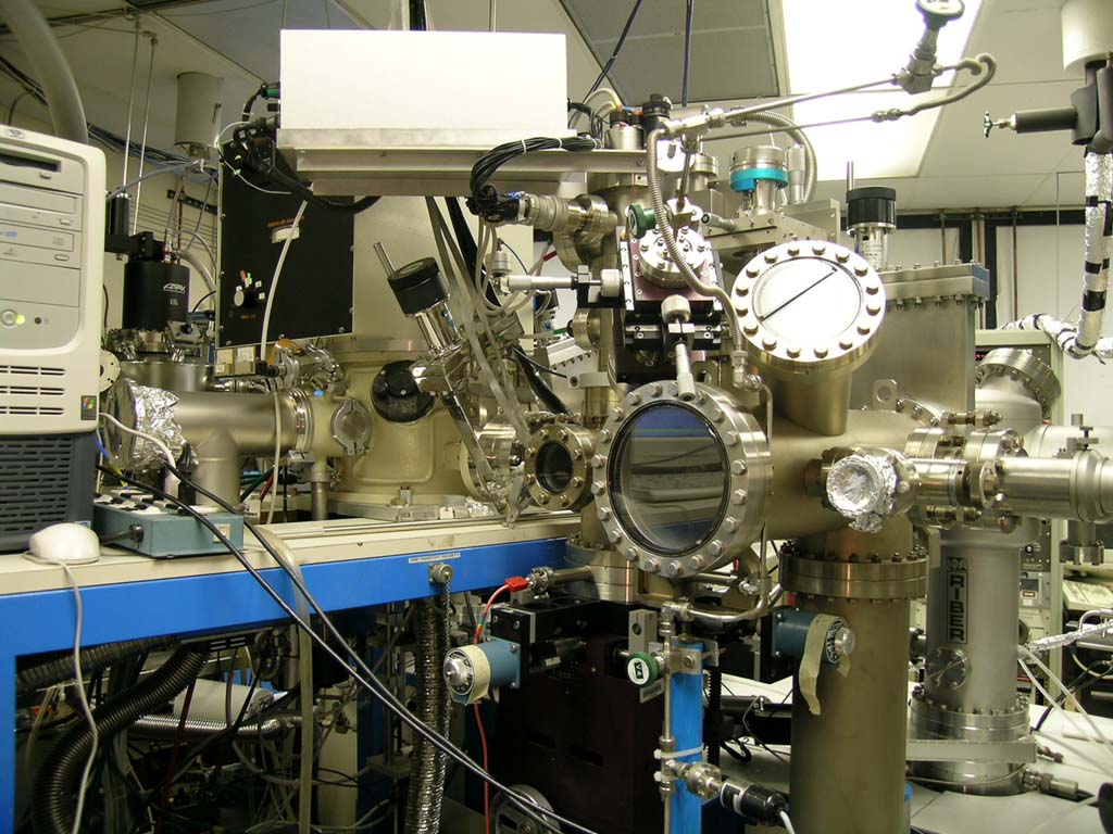
AFM-STM Chamber:
This chamber was the first system that integrates STM/AFM
that is UHV connected to an extensive growth and processing
system. A unique design consisting of suspended bellows
achieves vibration isolation of this chamber from the
rest of the system, a key engineering feat that has
enabled us to achieve atomic-resolution on III-V surfaces.
This chamber enables a morphological evolution studies
that look at effects of various types of growth or processing
while avoiding deleterious effects of ambient exposure.
An illustrative example is our studies on the kinetic
pathways of the InAs 3D island formation on GaAs (001).
Cleaning/Metallization/Dielectric
Chamber:
This chamber has quite diverse capability resulting
from three distinct equipment that are mounted: (1)
An electron-beam deposition system that allows deposition
of low vapor pressure materials such as W, Au, Si, fluorides,
oxides etc., (2) a gas-source cell containing a high-temperature
filament which is used for cracking of molecular gases,
and (3) standard Knudsen cells for deposition of low-vapor
pressure materials. The chamber also has RHEED analysis
capability. In our most recent work, we have extensively
used this chamber for semiconductor surface cleaning
using atomic hydrogen with a low thermal budget.
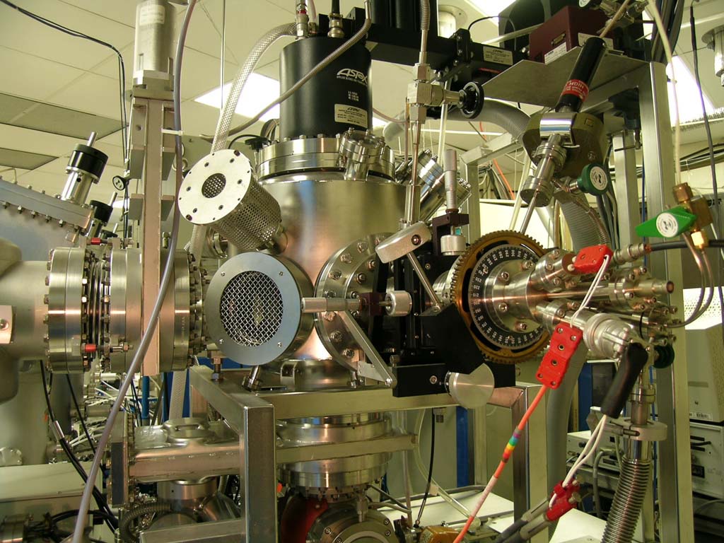
FIB Chamber:
The chamber is equipped with a liquid Ga ion gun and
a nozzle for reactive gas delivery. Nanoscale features
can be fabricated using Ga ions by either purely physical
sputtering or with sputtering assisted chemical etching.
The chamber is capable of patterning semiconductor as
well as dielectrics.
PECVD Chamber:
The chamber is used for deposition of SiO2 and Si3N4.
These dielectrics are typically used either as a mask
layer for further FIB patterning or as surface passivation
layers.
ECR Chamber:
The chamber uses an ECR source for the generation of
reactive ions. The gases connected to this chamber enable
etching of III-arsenides, Si, SiO2, and Si3N4. The chamber
has been designed so that spectroscopic ellipsometry
(SE) measurements can be performed to monitor the processes
in real-time.