I.1. Nanostructure Synthesis and Structure: Concepts and Implementation
A
large part of the Madhukar group's research in the past
two decades has focused on the molecular beam epitaxical
synthesis and structure of compound semiconductor (InGaAlAs)
heterojunction based low dimensional quantum structures
such as quantum wells, superlattices, quantum wires,
and quantum dots. A number of concepts and methodologies,
most of which have become common practice, were introduced
in our work. These include:
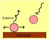
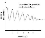
Use
of RHEED intensity behavior of static GaAs surface for
reproducible high quality in-situ preparation of buffer
layers for subsequent growth [I.1.9,12];
Growth interruption [I.1.18]
for realizing atomic level perfection in interfaces;
Alternate shuttering of molecular beams [I.1.33,34]
(later dubbed migration enhanced epitaxy, MEE) for realizing
high quality epitaxy at low growth temperatures;
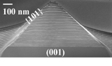
Substrate-encoded
size-reducing epitaxy (SESRE) [I.1.46,53,54,55]
for realizing quantum wire and box arrays of lattice
matched systems on structurally patterned substrates
via engineered surface stress directed self-assembly;
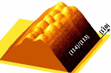
Intrinsic defect reduction in lattice mismatched epitaxy
via strain relief in growth over patterned substrates
(i.e.mesas) [I.1.35,36,53];
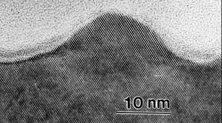
Discovery
of the existence of coherent (i.e. defect-free) three-dimensional
islands as a pathway for relief of strain in highly
strained epitaxy, the basis of the field dubbed self-assembled
quantum dots (SAQDs) [I.1.61];
Low temperature (<350°C) capping of islands using
MEE [I.1.66]; Improved
SAQD size uniformity via punctuated island growth (PIG)
[I.1.75]; Stress-directed
vertically self-organized growth of SAQDs [I.1.69];
Variable deposition approach (VDA) for independent manipulation
of SAQD density and size [I.1.73];
Controlled creation of coupled asymmetric SAQDs [I.1.74];
Engineered
surface stress driven spatially-selective self-assembly
of countable ensembles of lattice mismatch stress-induced
island quantum dots [I.1.85,86,87].
The above noted semiconductor nanostructure synthesis research in the Madhukar group utilizes the power of
a unique all-UHV interconnected system of six chambers comprising growth, in-situ patterning, etching, and characterization.
To learn more about the above noted contributions and continuing nanostructure synthesis research,
click on the bullets below. Or, go to Electronic Structure or Devices.
I.1(a) Atomic Scale Understanding of Lattice-Matched and Mismatched Epitaxy.
I.1(b) Growth-Controlled Self-Assembly of Epitaxical Nanostructures.
Current
Research Focus