I.1 Nanostructure Synthesis and Structure (continued)
I.1(b) Growth-Controlled Self-Assembly of Semiconductor Epitaxical Nanostructures:
The
Madhukar group is amongst the earliest groups to introduce
and refine in-situ creation of semiconductor quantum
wires and boxes utilizing purely growth-controlled approaches.
We pioneered the two purely growth-controlled approaches
to epitaxical semiconductor nanostructure synthesis
not requiring patterned features on the nanoscale and
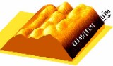
utilized world-wide today: (a) Growth on mesa tops of
structurally patterned substrates and [46,50,53-60]
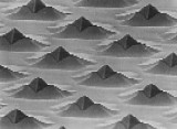
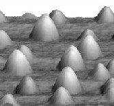
(b) Lattice-mismatch strain driven spontaneous formation
of defect-free 3-dimensional islands in highly strained
epitaxy [61,62,63,64-81].
The conceptual theme underlying these approaches derives from the understanding and manipulation of surface and
sub-surface spatially inhomogeneous stress that accompanies surfaces with curvatures, either pre-patterned or self-evolving. We have called this generic
approach "Surface Stress Engineering" and a specific usage SESRE (substrate-encoded size-reducing
epitaxy).