|
|
Structural
nature of InAs NCQDs on GaAs(001)
|
| This
work is supported by: DURINT-01
AFOSR Grant No. F49620-01-1-0474
|
|
Both
the integration schemes noted above require deposition
of the NCQDs on the semiconductor substrate. Therefore
we would like to know the structural and chemical nature
of the NCQDs in the as-deposited state. Given the NCQD
size the only viable technique for their studies is
high-resolution transmission electron microscopy (HRTEM).
Most of the previous TEM studies of NCQDs have been
performed when the NCQDs are deposited on amorphous
substrates such as the image shown in fig. 2 in the
introduction section. HRTEM studies on single crystal
semiconductor substrate are not a simple matter. For
imaging in plan-view geometry, the substrate thickness
needs to be below ~ 20nm to be able to image contrast
from NCQDs. Due to the fragility of the NCQDs, conventional
techniques for semiconductor thinning based on ion-beam
sputtering are not appropriate. We have therefore developed
and applied new techniques for the specimen preparation
based exclusively on chemical etching that are benign
and enable maintaining the integrity of the integrated
hybrid structures. A detailed account can be found in
reference 1. Figure 1(a) and (b) show a low magnification
TEM of an ensemble of InAs NCQDs on GaAs(001) and the
corresponding electron diffraction pattern, respectively.
The TEM image shows that the InAs NCQDs for dense close-packed
patches. The ring pattern from the NCQD ensemble in
fig. 1(b) reveals that the NCQDs are randomly oriented
on the substrate.
|
|
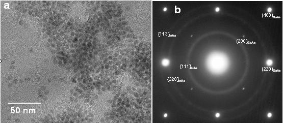
Figure 1 (a) Plan-view TEM image of InAs NCQDs on GaAs(001),
(b) corresponding electron diffraction pattern.
|
|
|
|
Figure 2 shows a HRTEM image
of a single NCQD. Lattice fringes from the {111} InAs
planes are clearly observed from the NCQD. The faint
vertical lines in the background are the lattice fringes
from the {220} GaAs substrate planes. Notice that there
is a dark halo, ~1-1.5nm thick, surrounding the InAs
NCQD. This thickness is consistent with the expected
thickness of the tri-octyl phosphine (TOP) surfactant
molecules that decorate the surface of the NCQDs in
the as-synthesized state. These molecules play a dual
role: (1) prevent coagulation of the NCQDs in the solution
and (2) provide passivation of the NCQD surface states.
Their presence suggests that there is no covalent bonding
between the NCQDs and the substrate thus explaining
their lack of any preferred orientation. For our intended
application, the presence of TOP is indeed necessary
so that the integrity of the NCQD luminescence is maintained
in the integrated hybrid structures.
|
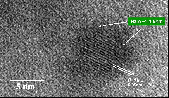 |
| Figure 2. HRTEM image on an
isolated InAs NCQD on GaAs(001).
|
References:
1. "Semiconductor nanocrystal quantum dots on single
crystal semiconductor substrates: High resolution transmission
electron microscopy", A. Konkar, S. Lu, A. Madhukar,
S. M. Hughes, and A. P. Alivisatos (accepted, to appear
in the May 2005 issue of Nano Lett.).
|
II.1
Study of Energy Transfer
II.3
Integrated Hybrid Nanostructures: Overgrowth on InAs NCQDs
DURINT
Project
- Nanocrystal/Eptaxial
2D integration
- Surface
Modification (Chemical & Biochemical)
- Nanoscale
Simultaneous Morphological & Optical Imaging
Back to Top
|