|
|
Integrated
Hybrid Nanostructures: Overgrowth on InAs NCQDs
|
|
This
work is supported by: DURINT-01
AFOSR Grant No. F49620-01-1-0474
|
Our
approach to epitaxical integration of NCQDs (schematically
shown in fig. 3 of the introduction) follows a four step
procedure:
1. Preparation of a fresh atomically
smooth GaAs(001) surface via MBE growth.
2. Deposition of NCQDs on the
substrate from the toluene solution in a controlled atmosphere
glove box.
3. Surface cleaning to remove
the organic moieties coming from the NCQD solution and
also the TOP ligand molecules from the NCQD surface.
4. High quality III-V epitaxical
overgrowth.
As a prototypical systemthe we have investigated epitaxical
integration of InAs NCQDs into GaAs matrix. Due to the
reduced thermal stability of the InAs NCQDs compared to
bulk InAs, a consequence of "Kelvin" effect,
steps 3 and 4 have to carried out with the lowest possible
thermal budget consistent with good quality overgrowth.
To minimize the thermal budget during step 3 we carry
out the cleaning with the assistance of H-radical flux.
And for step 4 we employ Migration Enhanced Epitaxy (MEE)
a special MBE based technique which allows high quality
epitaxy at low temperatures. Cleaning under optimized
conditions leads to substantial size-reduction of NCQDs,
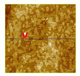
from ~ 4nm starting size to ~ 1nm. Figure 1 shows AFM
measurement of the NCQDs after optimized cleaning.
|
 |
|
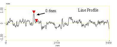 |
| Figure 1 (a)
AFM image of the NCQDs on GaAs(001) after H-assisted cleaning. (b) Height profile across the line
shown in panel (a).
|
|
To determine the quality
of the epitaxical overgrowth, the MEE growth is done
simultaneously on three types of substrates loaded on
the same holder:
(1) Untreated sample - this
sample is exposed only to the glove-box and serves as
the reference,
(2) Toluene exposed sample,
and
(3) InAs NCQD deposited sample.
The overgrowth consisted of deposition of 1ML InAs followed
by 170 ML of GaAs. The 1 ML InAs layer serves as an
marker to determine the optical quality.
HRTEM and PL studies
were performed to determine the structural and optical
nature of the overgrowth. The cross-sectional HRTEM
image shown in fig. 2 evidences the good structural
quality. Large regions of the sample were examined (compared
to the mean spacing between the NCQDs) and no extended
defects were observed. However, the limitations (spatial
resolution and lack of chemical information) of employed
TEM precludes observation of the embedded ~ 1nm InAs
NCQDs.
|
|
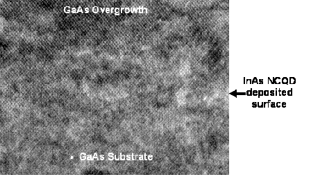
Figure 2 Cross-sectional HRTEM image of overgrowth
on InAs NCQDs.
|
| The
results from optical studies (see in figure 3) show that
the 1ML InAs PL of the toluene-exposed and NCQD-deposited
samples is comparable to that of reference, a result consistent
with the good structural quality. Though we do not see
a clear optical signature from the NCQDs, the NCQD deposited
sample shows a shoulder on the low-energy side of the
1 ML InAs PL peak. The location of this shoulder is qualitatively
consistent with that expected from sub-nm InAs NCQDs.
Following these encouraging results (for details see reference
1), we are proceeding with the obvious next step of using
InAs NCQDs with a larger starting size than the 4nm NCQDs
used in these studies. We have recently succeeded in synthesizing
8nm InAs NCQDs with large yield by using punctuated growth,
a concept that was developed and demonstrated in our lab
in the context of synthesizing the InAs self-assembled
quantum dots (SAQDs) with independent control over their
density and size (reference 2).
|
|
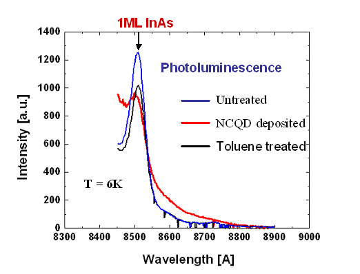
Figure 3 Photoluminescence behavior of the overgrowth
|
References:
1. "Integrated semiconductor nanocrystal and epitaxical
nanostructure systems: structural and optical behavior",
Anupam Madhukar, Siyuan Lu, Atul Konkar, Yi Zhang, Max
Ho, Steven M. Hughes, and A. Paul Alivisatos, Nano Lett.
5, 492 (2005).
2. "Punctuated island growth: An approach to examination
and control of quantum dot density, size, and shape evolution",
I. Mukhametzhanov, Z. Wei, R. Heitz, and A. Madhukar,
Appl. Phys. Lett. 75, 85 (1999)
|
II.1
Study of Energy Transfer
II.2
TEM Study
DURINT
Project
- Nanocrystal/Eptaxial
2D integration
- Surface
Modification (Chemical & Biochemical)
- Nanoscale
Simultaneous Morphological & Optical Imaging
Back to Top
|