|
|
Integrated
Epitaxical and Colloidal Nanostructure - Introduction
|
| This
work is supported by: DURINT-01
AFOSR Grant No. F49620-01-1-0474 |
| |
In
the past dozen or so years two classes of quantum dots,
the semiconductor self-assembled quantum dots (SAQD)
on a crystalline substrate such as InAs/GaAs (figure
1), Ge/Si, etc. [1,2] and the semiconductor nanocrystal
quantum dots (NCQDs) such as CdSe, InAs in solution
(figure 2) [3,4], have emerged as two independent and
dominant classes of quantum structures with considerable
potential for advancing nanotechnologies. Some of these
properties, largely for the epitaxical quantum dots,
have been well optimized and exploited to realize advanced
devices such as lasers [5,6], near to long wavelength
infra-red detectors [7], solid state amplifiers, resonant
tunneling diodes, etc.[2]. By contrast, the strength
and continuing predominant study and use of the NCQDs,
overwhelmingly II-VI, is in solution environments, such
as in biological luminescent labeling[8]. It is natural
then to ponder the potential of new phenomena and applications
that would follow from the integration of these two
fields. This is particularly so if the already sophisticated
III-V epitaxical semiconductor based optoelectronic
communication technology developed for the 0.98µm
to 1.5µm regime could be exploited. Towards
this end the canonical system to be examined is integration
of InAs based nanocrystal and the InAs/GaAs based epitaxical
nanostructure.
|
 |
 |
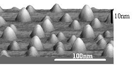
| Figure 1: AFM image of InAs epitaxical
island quantum dots grown on GaAs substrate
|
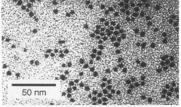
Figure 2 TEM image of InAs nanocrystal
quantum dots dispersed on carbon coated grid
|
| |
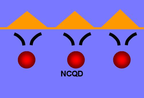
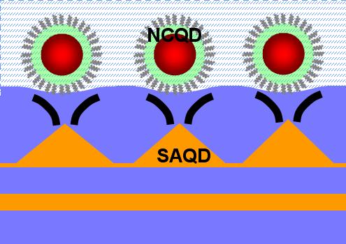
Our current
studies are focused on two pathways for the integration
of colloidal and epitaxial nanostructures: 1. epitaxical
overgrowth on chemically synthesized NCQDs and the buried
structure (figure 3) 2. NCQDs adsorbed on epitaxical
nanostructure (figure 4), their structural nature and
the communication between the NCQDs and underlying epitaxical
nanostructure.
|
|
|
|
Figure 3
|
Figure 4
|
Reference:
1. S.Guha, A. Madhukar and K. C. Rajkumar, Appl. Phys. Lett
57, 2110 (1990)
2. A. Madhukar, Ch.2 in "Nano-Optoelectronics", Ed.
M. Grundmann, Springer-Verlag, Berlin, (2002)
3. U. Woggon, "Optical Properties of Semiconductor Quantum
Dots", Springer-Verlag, Berlin, (1997)
4. A. P. Alivisatos, MRS Bulletin, 23, 18 (1998)
5. Q. Xie, A. Kalburge, P. Chen and A. Madhukar, IEEE Photon.
Technol. Lett. 8, 965 (1996)
6. NanoOptoelectronics, Ed. M. Grundmann, Springer-Verlag, berlin
(2002)
7. E. Kim, A. Madhukar, Z. M. Ye, and J. C. Campbell, App. Phys.
Lett. 84£¬3277 (2004) and references therein.
8. M. P. Bruchez, M. Moronne, P. Gin, S. Weiss, and A. P. Alivisatos,
Science, 281, 2013 (1998)
Details on this subject:
II.1
Study of Energy Transfer
II.2
TEM Study
II.3 Integrated Hybrid Nanostructures:
Overgrowth on InAs NCQDs
DURINT
Project
- Nanocrystal/Eptaxial
2D integration (Current Page)
- Surface
Modification (Chemical & Biochemical)
- Nanoscale
Simultaneous Morphological & Optical Imaging
Other research areas
I.Self-Assembled Semiconductor Epitaxical Quantum Nanostructures
III.Hybrid Biochemical / Inorganic Structures
Back to Research Focus
Back to top
|