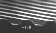
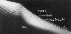
Growth
on structurally patterned substrates (SESRE)
By
structurally patterning the substrate appropriately,
the surface stress gradients can be made to induce spatially
preferred directions for the adatom surface migration
during deposition of even lattice matched overlayers,
including homoepitaxy. This, combined with exploitation
of the differences between adatom incorporation coefficients
on different crystallographic contiguous facets during
overlayer deposition on structurally patterned substrates,
allows spatially selective growth even for homoepitaxy
(such as GaAs on GaAs or Si on Si). This, in turn, allows
the creation of 2-dimensionally ordered arrays of single
or multiply stacked nanostructures, such as quantum
wires and quantum dots made of lattice matched materials
(GaAs/AlGaAs) [46,50,53,55]
as well as lattice mismatched materials (GaAs/InGaAs)
[55,56].


orientated along
2-fold As (2x4)